Open
PCB design

Posted by
Zarul Z.
Posted Wed, 16 Sept 2026

Posted by
Zarul Z.
Posted Wed, 16 Sept 2026
Budget
RM50
1 offer received so far
Location
Online
Completion Date
On Mon, 30 Nov 2026 (Anytime)
Duration
3 hours
Description
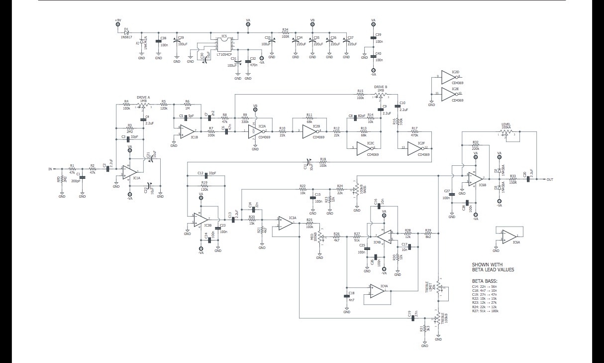
I am looking for a PCB design. Task Description: - Design a single-layer or simple double-layer PCB with basic components. - The primary function of the PCB will be signal processing and communication. - The design should incorporate a mix of through-hole and surface-mount components. - The final output required is Gerber files for manufacturing and assembly. Skills and Experience Required: - Proficiency in EasyEDA Pro for PCB design. - Experience in designing PCBs for signal processing and communication applications. - Knowledge of best practices for both through-hole and surface-mount component placement and routing. - Ability to generate accurate Gerber files for manufacturing.
Heroes Required
1
Clarify the details of the quest with the Citizen before making an offer.
No questions asked yet.